KARVIINTERCONNECTS
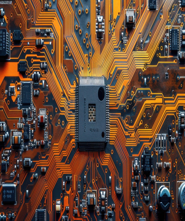
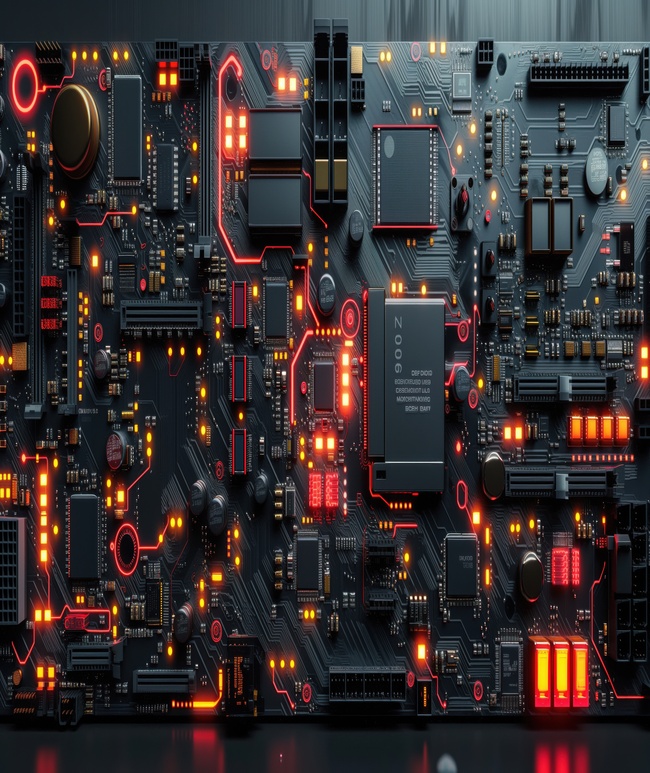
Design Your Board with No Limits
-
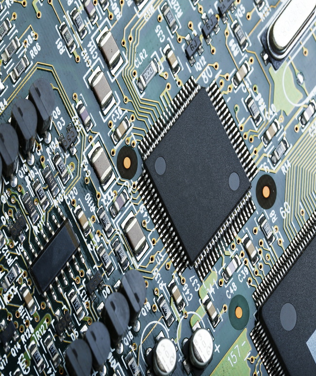
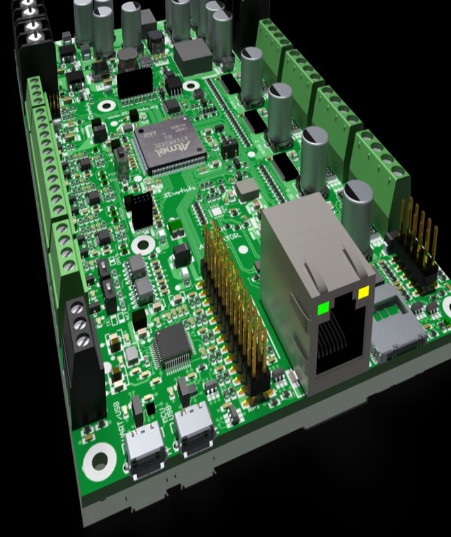
ATE Board Design
We provide specialized ATE (Automatic Test Equipment) PCB design services tailored for high-speed, high-reliability testing environments. -
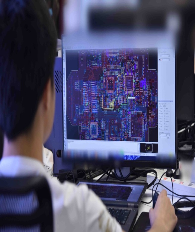
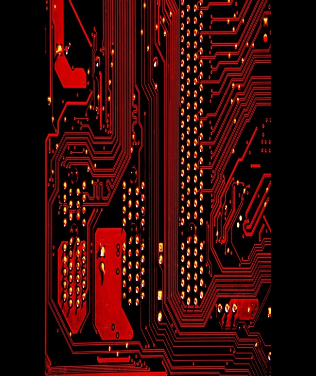
Analysis(SI/PI/Tharmal/EMI/EMC)
We offer advanced design analysis services to ensure your PCB performs flawlessly under real-world conditions. By integrating Power, Signal, Thermal, and EMI analysis -

Library Services
We deliver comprehensive solutions for the creation and maintenance of libraries that not only meet IPC 7351B Standards but also align with the unique specifications of our clients -
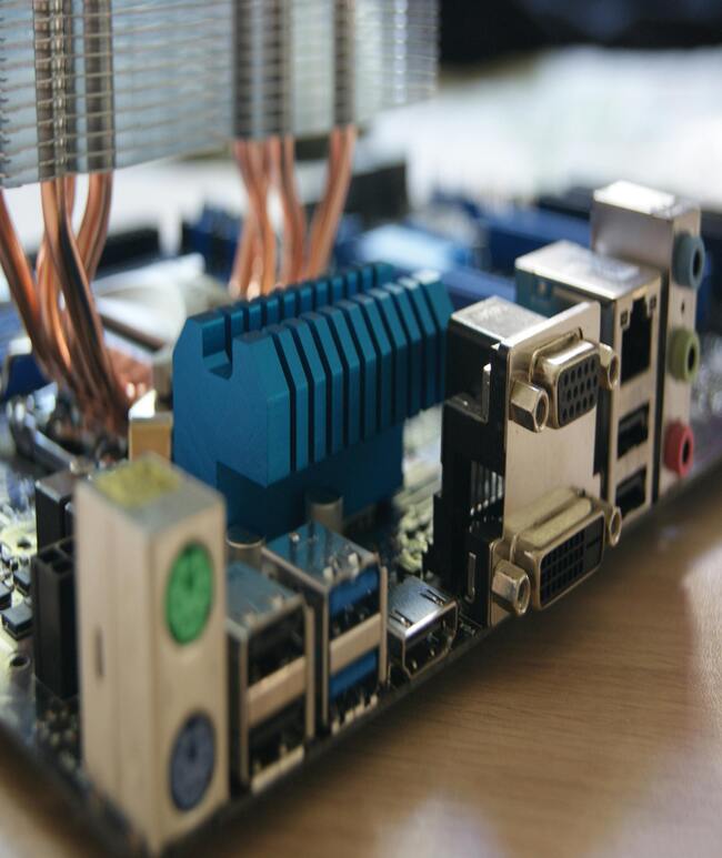
Mechanical Engineering
We go beyond circuitry. Our Mechanical Engineering Services ensure your designs are mechanically sound, thermally efficient, and manufacturable — with seamless integration into enclosures, housings, and real-world environments -
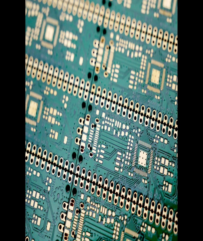
High-Speed Board Design
We specialize in High-Speed PCB Design for complex, high-performance systems where signal integrity, timing, and layout precision are critical -
Embedded HW Engineering
We provide end-to-end Embedded Hardware Engineering solutions that bring embedded systems to life — from architecture design and component selection to fully tested hardware ready for production -

Embedded SW Engineering Services
We offer full-stack Embedded Software Engineering Services — from low-level firmware to real-time operating systems (RTOS) and application layer development -

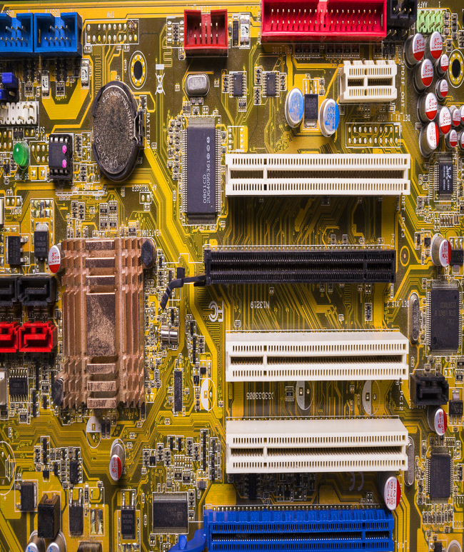
PCB FAB
We support you throughout the entire journey, including working directly with your preferred PCB fabrication and assembly vendors -
PCB Assembly
We actively support our customers through the entire PCB Assembly (PCBA) process, working directly with your chosen assembly vendors to ensure smooth production, functional quality, and timely delivery -

CAM Validation
we offer expert CAM (Computer-Aided Manufacturing) validation services to ensure your PCB designs are error-free, production-ready, and fully aligned with your fabrication vendor's capabilities -
Testing
we work closely with your chosen test or EMS vendor to ensure that your PCBs are thoroughly tested, validated, and meet performance expectations -
FCP(Flip Chip Package)
Flip Chip Packaging (FCP) is an advanced packaging technology where the semiconductor die is mounted face-down (flipped) directly onto the substrate using solder bumps -

SIP(System In Package)
System-in-Package (SiP) combines multiple semiconductor dies, passive components, and sometimes sensors or MEMS, all within a single package -
WBD(Wire Bond Design)
Wire bonding is a crucial process that connects the bond pads of a semiconductor die to the substrate or lead frame using fine wires (gold, aluminum, or copper) -
MCMC(Multichip Design)
Multi-Chip Module (MCM) design integrates multiple ICs within a single package or substrate, allowing them to operate together as a unified system -
CSP(Chip Scale Package)
Chip Scale Packaging (CSP) is an advanced semiconductor packaging approach where the final package is only slightly larger than the die itself — typically within 20% of the die footprint

The power of design help us to solve complex problems and cultivate business solutions.