KARVIINTERCONNECTS

Design Your Board with No Limits

ATE Board Design

  • ATE Board Design
  • ATE Board Design-2
  • ATE Board Design-3
Precision. Performance. Production-Ready.

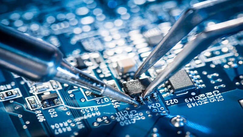
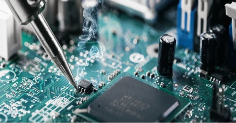
At KARVI INTERCONNECTS, we provide specialized ATE (Automatic Test Equipment) PCB design services tailored for high-speed, high-reliability testing environments. Our ATE PCBs are engineered to ensure accurate and repeatable testing across a wide range of applications — from semiconductor devices to fully assembled electronic products.

 
ATE PCB Design Capabilities
  • Custom Test Interface Board (TIB) Design
  • Load Board & Probe Card Development
  • High-Density PCB Layouts for Test Fixtures
  • Controlled Impedance & Length Matching
  • Design for In-Circuit Test (ICT) & Functional Test (FCT)
  • Boundary Scan / JTAG Integration
  • Signal Integrity & Power Integrity Optimization
  • Pogo Pin & Bed-of-Nails Fixture Compatibility
  • Mechanical and Thermal Design Considerations
Applications

Our ATE PCB designs are used in:

  • Semiconductor Device Testing
  • Automotive ECU & Sensor Testing
  • Telecom & RF Module Validation
  • Medical Device Functional Testing
  • Consumer Electronics Board-Level Testing
Why Choose Us for ATE PCB Design?
  • Expertise in High-Speed, High-Pin-Count PCBs
  • Proven Track Record in Production Test Environments
  • Close Collaboration with Test Fixture Vendors
  • Fast Turnaround & DFM/DFT-Compliant Designs
  • Integration with Popular ATE Platforms (Teradyne, Advantest, SPEA, etc.)
From Concept to Production

We handle the entire ATE board design cycle:

  • Requirements Analysis
  • Schematic & Layout Design
  • Mechanical Fixture Alignment
  • Signal Integrity Simulation
  • Manufacturing Support & Review