KARVIINTERCONNECTS

Design Your Board with No Limits

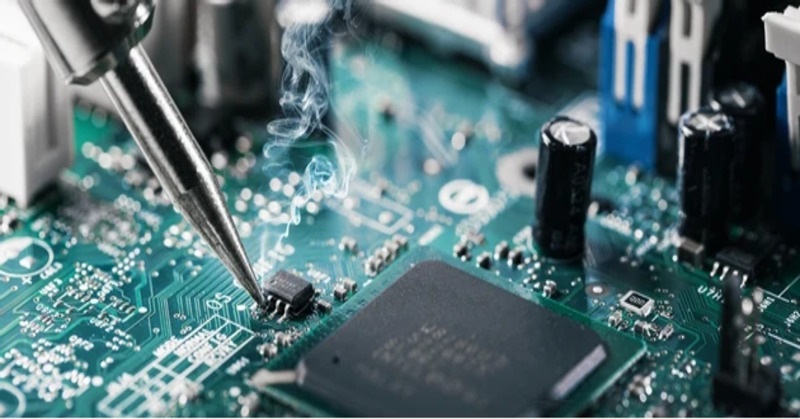
Flip Chip Package (FCP) Design

  • ATE Board Design
  • ATE Board Design-2
  • ATE Board Design-3
Advanced Package Design for High-Performance ICs

Flip Chip Packaging (FCP) is an advanced packaging technology where the semiconductor die is mounted face-down (flipped) directly onto the substrate using solder bumps. This eliminates the need for bond wires, enabling:

  • Shorter electrical paths
  • Better thermal conduction
  • Higher frequency operation
  • Smaller package sizes

Flip chip is widely used in high-speed processors, GPUs, FPGAs, ASICs, RF ICs, and high-performance mixed-signal devices.

 
Die-to-Substrate Interconnect Planning
  • Solder bump pattern design (C4 bumps, micro-bumps)
  • Die bump assignment and net routing
  • Underfill selection and bump pitch optimization
  • Co-design of RDL layers and bump redistribution
Substrate Design & Layout
  • Multi-layer organic substrate design
  • Escape routing for high-density I/Os
  • Power/Ground plane structure and decoupling
  • Ball Grid Array (BGA) mapping and signal breakout
Electrical, Thermal & Mechanical Analysis
  • Signal and Power Integrity (SI/PI) simulations
  • Thermal modeling for high-power flip chip modules
  • Warpage and stress analysis during reflow
  • Die attach, lid design, and TIM (thermal interface material) considerations
Design Toolchain & Co-Design Support
  • Tools: Cadence Allegro, ANSYS SIwave, Mentor Xpedition
  • Integration with silicon, substrate, and PCB design flows
  • Foundry and OSAT collaboration for process compatibility
  • Package-level LVS and DRC validation
FCP Applications We Support
  • High-speed networking ICs (SerDes, PHYs)
  • AI & ML processors, SoCs, and GPUs
  • Automotive radar and ADAS ICs
  • 5G, RF front-end modules
  • Medical and aerospace-grade custom ASICs