KARVIINTERCONNECTS

Design Your Board with No Limits
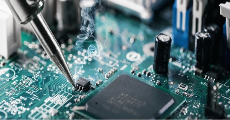
Wire Bond Design

  • Library Services
  • Library Services
  • Library Services
Reliable Interconnects for Advanced IC Packaging

Wire bonding is a crucial process that connects the bond pads of a semiconductor die to the substrate or lead frame using fine wires (gold, aluminum, or copper). This process enables precise electrical connectivity, robust mechanical strength, and efficient thermal transfer within integrated circuit (IC) packages.

 
Bond Pad and Wire Layout
  • Accurate bond pad placement and pitch control
  • Optimized wire loop profiling for consistent performance
  • Support for gold, aluminum, and copper bonding wires
  • High-density and fine-pitch wire bonding layouts
Electrical and Mechanical Considerations
  • Signal integrity and crosstalk mitigation
  • Loop height and sweep optimization to prevent shorts
  • Stress analysis for wire durability and reliability
  • Thermal analysis for high-power and heat-sensitive packages
Process & Manufacturability Support
  • DFM checks for wire bond compatibility
  • Coordination with OSATs and assembly vendors
  • Bond pad and test structure design for quality validation
  • Support for standard and advanced processes (ball, wedge bonding)
Applications Supported
  • ASICs, SoCs, and memory devices
  • Power modules and analog ICs
  • RF and mixed-signal devices
  • Sensor packages and MEMS
  • Automotive, industrial, and medical-grade electronics